A Practical Analysis
This article welcomes anyone that wants to help with translations or contributions.
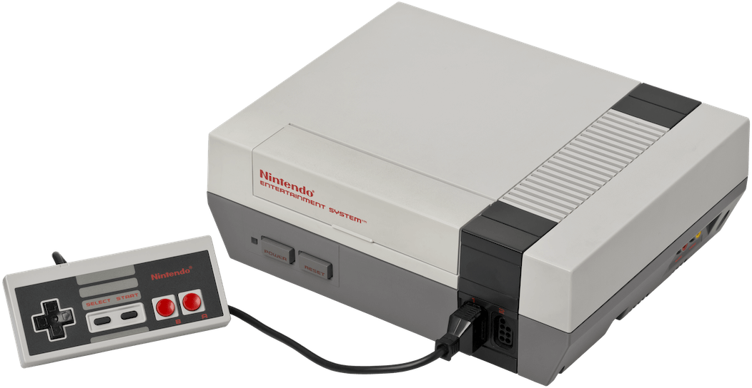
The NES, released on 18/10/1985 in America and 01/09/1986 in Europe
A quick introduction
At first glance, the NES can be considered just another 6502 computer with a sophisticated case and a controller.
And the fact is, this is technically right, but let me show you why the CPU will not actually be the central part of this system.
CPU
The NES’s CPU is a Ricoh 2A03, which is based on the popular 8-bit MOS Technology 6502 and runs at 1.79 MHz (or 1.66 MHz in PAL systems).
A bit of context
The CPU market in the late 70s and early 80s was quite diverse. If any company wanted to build an affordable microcomputer, the following options were available:
- The Intel 8080: A popular CPU featured in the Altair, the first ‘personal’ computer. It has an 8-bit data bus and a 16-bit address bus.
- The Zilog Z80: An ‘unofficial’ version of the 8080 enhanced with more instructions, registers and internal components. It was sold at a cheaper price and could still execute 8080 programs. Amstrad and Sinclair where some of the companies that chose this CPU.
- The Motorola 6800: Another 8-bit CPU designed by Motorola, it contains a completely different instruction set. Many do-it-yourself computer kits, synthesisers and all-in-one computers included the 6800.
As if wasn’t enough, another company with the name MOS appeared on the market and offered a redesigned version of the 6800 called 6502. While incompatible with the rest, the new chip was much much less expensive to produce and it was a matter of time before most of the famous computer makers (Commodore, Apple, Atari, Acorn and so forth) chose the 6502 to power their machines.
Back in Japan, Nintendo needed something inexpensive but familiar to develop for, so they selected the 6502. Ricoh, their CPU supplier, successfully produced a 6502-compatible CPU by licensing the chip designs from MOS and subsequently making some modifications here and there (we’ll go over the details later on).
Memory
The system provides 2 KB of Work RAM (WRAM) for storing variables.
The components of the system are memory-mapped, meaning that they are accessed using memory addresses. The memory space is composed of the Program ROM, WRAM, the PPU, the APU and 2 controllers, each component is explained throughout this article.
Scrapped functions
The Ricoh 2A03 happens to omit the Binary-coded Decimal or ‘BCD’ mode originally included in the 6502. BCD enables to encode each decimal digit of a number as a separate 4-bit binary, and since the 6502 uses 8-bit words, each word stores two decimal digits.
As an example, the decimal number ‘42’ is:
- ‘0010 1010’ in binary.
- ‘0100 0010’ in BCD.
- Since ‘0100’ translates to ‘4’ and ‘0010’ translates to ‘2’.
This mode is useful for applications that require treating each decimal place separately (for instance, a digital clock). However, it requires more storage since each word can only encode up to the decimal number ‘99’ (where as traditional binary can encode up to ‘255’).
In any case, Ricoh deliberately broke BCD mode in its chip by severing the control lines that activate it. This was presumably done in an effort to avoid paying royalties to MOS, since BCD was patented by them (and the necessary legislation to copyright integrated circuit layout in the United States wasn’t enacted until 1984).
Graphics
Graphics are generated by a proprietary chip called the Picture Processing Unit or ‘PPU’ for short. This chip renders sprites and background graphics, outputting the result to the video signal.
Constructing the frame
As with its contemporaries this chip is designed for the behaviour of a CRT display. There is no frame-buffer as such: the PPU will render in step with the CRT’s beam, building the image on-the-fly.
Additionally, the frame that the PPU outputs is built using two different layers. For demonstration purposes, Super Mario Bros will be used as example to show how this works:
Tiles Found in its Character ROM
(For demonstration purposes a default palette is being used)
The PPU uses tiles as a basic ingredient for producing sprites and backgrounds.
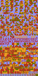
The NES defines tiles as basic 8×8 maps stored in Character Memory (found in the cartridge). Each pixel of the tile uses one of four colours (their palettes are defined later).
Four Tiles are combined in 16×16 maps called blocks where they have to share the same colour palette.
In order to start drawing the picture, the PPU first looks for tile references from a different set of tables previously populated by the game. Each table is used to build a layer of the frame.
Secrets and Limitations
If you’re thinking that a frame-buffer system with memory allocated to store the full frame would have been preferable: RAM costs were very high and the console’s goal was to be affordable. This design proved to be very efficient and flexible too!
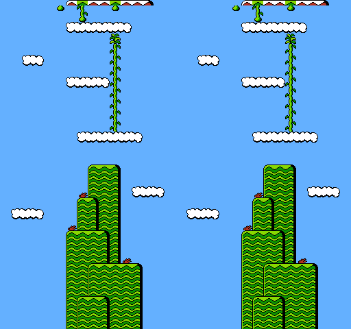
Super Mario Bros 2
Nametable setup for vertical scrolling (Horizontal Mirroring)
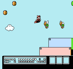
The character has to climb the mountain, the viewable area is at the bottom while the PPU has time to render the top.Super Mario Bros 3
Mario can run and fly, so the PPU needs to scroll diagonally
Notice the right edge showing the wrong colour palette
The left edge has a mask applied
Some games require the main character to move vertically, thus the Nametable will be set up with Horizontal Mirroring. Other games want their character to move left and right, then Vertical Mirroring is used instead.
The specific type of mirroring will allow the PPU to update background tiles without the user noticing: There is plenty of space to scroll while new tiles are being rendered at distance.
But what if the character wants to move diagonally? The PPU can scroll in any direction, but without extra VRAM, the edges may ended up having to share the same colour palette (remember that tiles are grouped in blocks).
This is why some games like Super Mario Bros 3 show strange graphics at the right edge of the screen while Mario moves (the game is set up for vertical scrolling). It’s possible that they needed to keep the costs down regarding the amount of hardware needed in the cartridge (This game has already a powerful mapper installed).
As an interesting fix: the PPU allowed to apply a one vertical mask on top of tiles, effectively hiding part of the glitches.
Audio
A dedicated component called Audio Processing Unit or ‘APU’ for short provides this functionality. Ricoh embedded it inside the CPU chip to avoid unlicensed cloning of both CPU and APU.
This audio chip is a Programmable Sound Generator (PSG), which means that it can only produce pre-defined wave-forms. The APU has five channels of audio, each one is reserved for a specific wave-form. The music data is found in the Program ROM.
Each wave-form contains different properties that can be altered to produce a specific note, sound or volume. These five channels are continuously mixed and sent through the audio signal.
Let’s now discuss the type of wave-forms synthesised by the APU:
Mother (1989)
Pulse waves have a very distinct beep sound that is mainly used for melody or sound effects.
The APU reserves two channels for one pulse-wave each. These channels use one of three different voices by varying its pulse-width.
Most of the games use one pulse channel for melody and the other for accompaniment.
When the game requires to play a sound effect, the accompaniment is switched to play the effect and then returns to accompanying, this avoids interrupting the melody during gameplay.
Secrets and Limitations
While the APU was not comparable to the quality of a Vinyl, Cassette or CD, programmers did find different ways of expanding the capability thanks to the modular architecture of this console.
Castlevania III (1989)
The Japanese model of the NES, the Famicom, provided exclusive cartridge pins available for sound expansion, games like Castlevania 3 included the Konami VRC6 chip, which allowed two extra pulse waves and a sawtooth wave.
Check out the difference between the American version (which didn’t have capabilities for sound expansion).
Games
They are mainly written in 6502 assembly language and reside in the Program ROM while its graphics (tiles) are stored in the Character Memory.
The 16-bit address space limits the system to 64 KB of addressable memory. The system I/O is memory mapped, that only leaves around 8 KB of available storage for the program. If a game required extra space, extra chips (mappers) would be included in the cartridge, with an attendant increase in production costs.
Some cartridges included an additional battery-backed WRAM to store saves.
Anti-piracy & Region Lock
Nintendo was able to block unauthorised publishing thanks to the inclusion of a proprietary Lockout chip called Checking Integrated Circuit or CIC, it’s located in the console and is connected to the reset signals (and is not easily removed).
This chip runs 10NES, an internal program that checks for the existence of another Lockout chip in the game cartridge, if that check fails then the console is sent into an infinite reset.
Both lockout chips are in constant communication during the console’s uptime. This system can be defeated by cutting one of the pins on the console’s Lockout, this leaves the chip in an idle state. Alternatively, sending it a -5V signal can freeze it.
The CIC exists as a result of the fear caused by the video game crash of 1983. Nintendo’s then president Hiroshi Yamauchi decided that in order to enforce good quality games they would be in charge of approving every single one of them. You’ll notice that the Japanese model of the console, the Famicom, was in fact released before this event happened, that’s why the CIC circuitry is used for sound expansions instead.
Sources / Keep Reading
General
CPU
- Ricoh 2A03
- MOS Technology 6502
- 6502 Binary-coded decimal (BCD) mode
- Difference between 6502 and 2A03 CPU core
- Semiconductor Chip Protection Act of 1984
- Radio Electronics Magazine December 1977, Page 86
- Radio Electronics Magazine August 1981, Page 76
- How much did the 6502 and Z80 cost? (Retrocomputing)
Graphics
- Nametables
- Attribute Tables
- Object Attribute Memory (OAM)
- N3s’ detailed explanation (Archived)
- Retro Game Mechanics Explained, an interesting Youtube Channel
Audio
Games
Photography
- Motherboard and console: Evan Amos Gallery
- Diagrams and game screenshots: Me
Contributing
This article is part of the Architecture of Consoles series. If you found it interesting please consider donating, your contribution will be used to get more tools and resources that will help to improve the quality of current articles and upcoming ones.


A list of desirable tools and latest acquisitions for this article are tracked in here:
## Interesting hardware to get (ordered by priority)

- NTSC NES or JAP Famicom (only if found at a reasonable price)
- NESRGB kit (still very expensive, may be better to wait for that)
- Any development cart out there (only if found at a reasonable price)
Alternatively, you can help out by suggesting changes and/or adding translations.
Changelog
Always nice to keep a record of changes.
## 2020-08-23

- Added some historical context to the CPU section
- Corrected assumptions about the lack of BCD, thanks @danweiss and @konrad
- (Main diagram) Removed CPU connection to Character RAM, thanks @danweiss

## 2020-06-13

- Added mention to OAM DMA

## 2020-06-06

- Expanded BCD mode
- Redesigned main diagram (the NES diagram was the first one for this site, since then the style evolved a lot!)

## 2019-09-17

- Added a quick introduction

## 2019-04-06

- Corrected wrong explanation about tile glitches

## 2019-02-17

- Fixed Grammar
- Replaced images and videos with better quality ones.

## 2019-01-25

- Improved first draft with the help of @dpt
- Ready for publication
