A Practical Analysis
This article welcomes anyone that wants to help with translations or contributions.
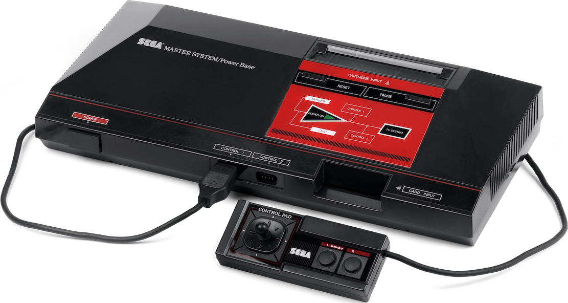
The Sega Master System
Released on 20/10/1985 in Japan, 09/1986 in America and 06/1987 in Europe
A quick introduction
The Master System comes from a long line of succession. What started as a collection of off-the-shelf components, has now gained a new identity thanks to Sega’s engineering.
Models and variants
I was a bit confused at first while reading about the different models that Sega ended up shipping, so here is a summary of the main models discussed to avoid further confusions:
- Sega Mark III: The first console featuring this architecture, only released in Japan.
- Sega Master System (Europe and America): A rebranded Mark III with a new case, a BIOS ROM chip and a different cartridge slot.
- Sega Master System (Japan): An European/American Master system with the Mark III’s cartridge slot, a new FM chip and a jack port for ‘3D glasses’. However, it lacks the
RESETbutton.
From now one I’ll use the term ‘Master System’ or ‘SMS’ to refer to all of these, except when talking about exclusive features from a particular model.
CPU
Sega decided on a fully-fledged Zilog Z80 CPU running at ~3.58 MHz. A popular choice by other machines like the ZX Spectrum and the Amstrad CPC. The Z80 has an instruction set compatible with the Intel 8080 but expanded with lots of more instructions.
The motherboard picture at the start of the article shows a NEC D780C-1 CPU, that’s just SEGA second-sourcing the chip to different manufacturers, other revisions even included the chip manufactured by Zilog. But for this article, it doesn’t matter who fabricated the CPU, as the internal features remain the same.
Memory available
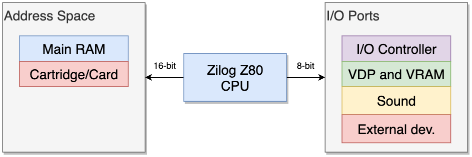
The Z80 has a 16-bit address bus, so the CPU can find up to 64 KB worth of memory. In the memory map you’ll find 8 KB of RAM for general purpose use, this is mirrored in another 8 KB block. Finally, up to 48 KB of game ROM are mapped as well.
Accessing the rest of the components
As you can read from the previous paragraph, only main RAM and some cartridge ROM is found on the address space, so how can the program access other components? Well, unlike Nintendo’s Famicom/NES, not all the hardware of the Master System is mapped using memory locations. Instead, some peripherals are found on the I/O space.
This is because the Z80 family contains an interesting feature called I/O ports which enables the CPU to communicate with other hardware without running out of memory addresses. For this, there’s a separate address space for ‘I/O devices’ called ports and both share the same data and address bus. The difference, however, is that ports are read and written using IN and OUT instructions, respectively – as opposed to the traditional load/store instruction (LD).
When an IN or OUT instruction is executed, the Z80 sets up the address lines pointing to the peripheral (which could be, for instance, a keyboard), flags its IORQ pin indicating that an I/O request has been initiated and also flags the RD pin or the WR pin whether it’s an IN or OUT instruction, respectively. The addressed peripheral must manually check for the address bus and the I/O pins and perform the required operation. In the case of an IN instruction, the CPU will store the received value on a pre-defined register.SMS’ Addressing layout
The way SEGA interconnected the CPU with the rest of the components enables not only to access values, but also showing/hiding certain components from appearing in the memory map.
Curiously enough, the Game Boy had a Z80 ‘variant’ that completely omitted the I/O ports. Thus, it had to fit everything in the memory map.
Backwards compatibility
The architecture of this console is very similar to its predecessor, the Sega SG-1000, so the Master System managed to gain backwards compatibility with the SG-1000. Although, this only applies to the Japanese variant since the others contain a different cartridge slot.
Graphics
The drawings on the screen are produced by a proprietary chip called Video Display Processor or ‘VDP’. Internally, it has the same design of the Texas instrument TMS9918 (used in the SG-1000), but enhanced with more features which we will discuss in the following sections.
Organising the content
Memory architecture of the VDP
Next to the VDP is connected 16 KB of VRAM which only the VDP can access using a 16-bit data bus. If you look at the motherboard picture again, you’ll notice that both RAM and VRAM chips are roughly the same, except that VRAM uses the chip model ending in ‘20’ which has lower latency.
In the case of the Master System, VRAM houses everything the VDP will require for rendering (except Colour RAM). The CPU fills VRAM by writing on VDP’s registers, which will in turn forward the values to VRAM. Since the VDP is accessed using I/O ports, the CPU must use IN and OUT instructions.
Constructing the frame
The VDP renders frames with a resolution of up to 256×192 pixels, further revision added support for 256×224 px and 256×240 px, however, to maintain compatibility with all models, developers held on to the standard resolution. This chip has the same modus operandi of Nintendo’s PPU, in other words, graphics are rendered on-the-spot.
On the other side, the VDP has four different modes of operation which will alter the characteristics of the frame (colour depth and resolution):
- Mode 0 to III: Inherited from the TMS9918 found on the SG-1000. Included for backwards compatibility, although any SMS game can use them.
- Mode IV: Native mode of the Master System, which enables access to all the state-of-the-art features of the VDP. For the analysis, we’ll focus on this one!
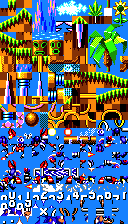
Now let’s see how a frame is drawn step by step, for this, I’ll borrow Sonic The Hedgehog’s assets. Also, to make explanations easier, I’m going to focus on the standard memory layout that Sega suggest for organising the graphics content (just remember that the VDP is very flexible with this, so games are allowed to optimise it).
Tiles Found in VRAM
Mode IV is based on the tile system. To recall previous explanations about tile engines, tiles are just 8×8 pixel bitmaps which the renderer fetches to draw the game’s graphics. In the case of the VDP, the frame is composed of two planes, the background layer and the sprite layer.
Inside VRAM, there’s an area dedicated for tiles called Character generator (Sega calls ‘Characters’ to tiles) and it’s set to be 14 KB long. Each tile occupies 32 bytes, so we can store up to 448 tiles.
There are 64 pixels defined on every tile, the VDP rules that each pixel must weight 4 bits, that means that up to 16 colours can be chosen. Those bits reference a single entry on Colour RAM or ‘CRAM’. That area is found inside the VDP and stores the colour palettes. Colour palette systems help reduce the size of tiles in memory and allows programmers to alternate its colours without storing multiple copies.
Colour RAM stores two palettes of 16 colours each. Each entry is 6-bit wide and each 2-bit set defines one colour from the RGB model. This means that there are 64 colours available to choose from.
Secrets and limitation
At first glance, the VDP may seem like another chip with minimal functionality that we now take for granted. Although, it happened to divert a lot of attention from Nintendo’s offering at that time. So, why would that be?
Well, first of all, the VDP was able to tell if two sprites were colliding. This was done checking its status register. It couldn’t detect which ones in particular, but that limitation was tackled by reading other registers as well, like the scan-line counter one. You can imagine it as a method of ‘triangulation’.
This feature is not new actually, as the TMS9918 also included it, thus the SG-1000 had collision detection too.
Video Output
The video-out connector of this system is incredibly handy. It exposes composite and RGB signals, which can be imagined as the two ‘extremes’ of video quality.
On the downside, it doesn’t carry ‘composite sync’, so making use of the RGB will require to capture the sync signal from composite, and its quality isn’t optimal.
Audio
The audio capabilities of this console are pretty much aligned with the rest of the 80s equipment. Inside the VDP chip, we find a slightly-customised version of the Texas Instruments SN76489, which is a Programmable Sound Generator or ‘PSG’. This is the same type used for the NES/Famicom, albeit having different functions.
A PSG can only synthesise a limited set of waveforms, each channel allocates a single waveform. I’ve previously introduced some PSGs on the NES article and the Gameboy if you want to read more about this type of sound synthesis.
With the SMS, the PSG is programmed by altering its set of external registers using the aforementioned I/O ports.
Now let’s take a look at each type of waveform the SN76489 can generate:
Sonic The Hedgehog (1991)
Pulse/Tone waves produce that iconic sound from the 8-bit generation. The sound wave is generated by latching up the voltage, keeping it steady and then dropping it altogether. Repeat this at a constant rate and a tone will be heard.
The period of the wave will define the frequency of the sound (musical note). Its duty cycle affects the timbre.
All of this is handled by the PSG, which can produce three pulse waves at the same time. The SN76489 in particular exposes a 10-bit counter on each channel that will be used internally to latch at a high rate, resulting in a pulse wave at a programmable frequency.
Secrets and limitations
Just like the VDP, the PSG is a no-brainer, but it does hide some interesting functionality:
Tap to enable interactionDouble Dragon (1987)
The Japanese version of the Master System embedded an extra chip for audio made by Yamaha called YM2413. It’s drastically different from the previous PSG as it uses the frequency modulation technique to generate sound. I’ve explained briefly how this works in the Mega Drive article, in case you are interested.
This chip in particular has nine channels of audio. Each channel can either select one of the 16 preset instruments, or define a custom one by programming the carrier and modulator. Unfortunately, only one custom instrument is allowed at a time. On the other side, the new instrument provides some interesting functions, such as ADSR envelope controls and feedback.
The YM2413 has also a second mode of operation called Rhythm mode which instead provides six channels supplemented with five extra channels for rhythm instruments only.
The final sound output is generated by the YM2413, which mixes its own channels along with the PSG ones.
The Mark III version didn’t include this chip, but FM was available as an expansion unit called FM Sound Unit. The rest (European and American Master Systems) had to stick with the PSG, although some third-party installations eventually appeared.
I/O
Like the other systems from its generation, the CPU is mostly in charge of handling I/O. In this case, the Z80 processor is unique for having that special I/O addressing, but still, there will be CPU cycles spent in moving bits around components.
On the other side, the SMS uses a dedicated I/O controller chip to not only interface the joypads, but also enabling and disabling parts of the system, which will alter the address map. Furthermore, this controller is essential for supporting the FM expansion, since the FM’s exposes ports which conflict with the rest of the system (that is, without the intervention of the I/O chip).
Available interfaces
Apart from the two controller ports, the system contains one proprietary cartridge slot, one ‘Sega Card’ slot and one expansion slot reserved for ‘future accessories’. The latter was never used, except for the FM expansion in the Mark III. Even so, the SMS and Mark III had a different expansion port design.
Top interruptors
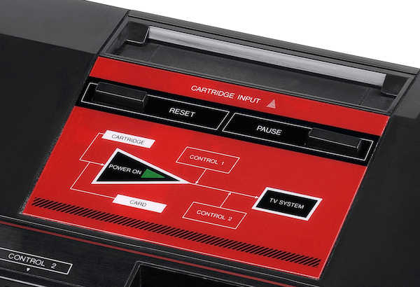
Another speciality about this console is that includes two buttons on the top of its case, PAUSE and RESET, you can guess what they do!Top of the case
When the PAUSE button is pressed, a non-maskable interrupt is sent to the CPU, the interrupt vector is stored in the game itself. This means that it’s up to the game to honour the press.
By contrast and for some strange reason, the RESET button is handled like a keypress on the controller.
Operating System
There’s a small 8 KB BIOS ROM fitted on the motherboard that gets executed whenever the console is turned on. The program itself doesn’t fit into the category of an ‘Operating System’, it’s more of a Boot Manager.
Medium selector
The main goal of the BIOS is to bootstrap a valid game from either game slot in the following priority: The Sega Card, the cartridge and the expansion module.
The boot process works as follows:
- Copy part of its code to main RAM.
- A crucial step since the program will start manipulating I/O ports, which will at some point disable access to the ROM!
- Show splash screen (Only in USA/Europe).
- Check each slot for a valid game.
- This is done by talking to the I/O controller chip to activate the required section, then copying the game header (16 bytes) from each slot to check if the game content is valid. The header must have
TMR SEGAencoded.
- This is done by talking to the I/O controller chip to activate the required section, then copying the game header (16 bytes) from each slot to check if the game content is valid. The header must have
- Perform a region check.
- Boot up the game
Surprise screen
If any of the checks fails, the console will loop indefinitely while showing a screen that prompts the user to insert a valid game.USA/Europe error message (after the initial splash)Japanese ‘error’ message (enhanced by the FM chip!)
As you can see, there’re some creative differences between regions. The first time I heard the Japanese one I thought it came from Electric Light Orchestra (the band), but it’s actually from Space Harrier (the game). Also, the perspective effect on the floor is accomplished by altering the colour palettes.
More regional differences
Because the Japanese variant was backwards compatible with the SG-1000, the header check is replaced with an ‘integrity check’ that instead reads data from the first 256 bytes multiple times to detect if it’s garbage.
Furthermore, the Mark III doesn’t have a BIOS, so the slots are activated with hardware switches and the cartridge is the one given priority.
Updatability and later BIOS chips
The BIOS ROM, by its nature, is not updatable. Although, as new console revisions entered the market, it was discovered that Sega also updated the BIOS program.
Later ones even embedded a whole game! As a consequence, the ROM chip got bigger and was accompanied by a dedicated mapper.
Games
To make a long story short, games are written in plain Z80 assembly, that’s it. If you’ve been reading articles of later consoles, there are no compilers or assisting software here (apart from the assembler).
Medium
The Master Systems provides two different mediums for distributing games:
- The Cartridge: Most common one, up to 48 KB of memory can be addressed. However, by including a mapper, the system can access a wider space and/or handle other chips like RAM which can be used to store saves.
- Sega provided official mappers for developers called ‘Paging Chips’, the most powerful one could map up to 512 KB of memory!
- The Sega Card: Has a very thin case and it’s cheaper to manufacture. Up to 32 KB of memory can be addressed. Since SEGA never designed a mapper for this medium, the largest card found in the market contained a 32 KB ROM.
Anti-Piracy and Region locking
Unlike Nintendo, Sega didn’t employ aggressive methods to control the distribution of their games, they did however prevent American and European systems from running Japanese games by altering the shape of the cartridge slot and using a different ROM header check.
On the other side, American and European systems had to include the aforementioned TMR SEGA code on their header. So I supposed this enabled them to prevent unauthorised distribution by making use of trademark laws.
That’s all folks
Having previously written the Nintendo DS article really puts into perspective how complicated tech has become. The Master System is very straightforward in that sense, even after some ‘technical nitpicking’ that I may have said here and there.
Anyway, I hope this article helped you get an overall impression of the state of technology of the early-to-mid-80s. I also want to thank the smspower.org community and the /r/Emulation discord for reading the first draft and pointing out lots of mistakes and suggestions.
Until next time!
Rodrigo
This article has been dedicated to the memory of Jacinto ‘Pocho’ Fornasier.
Sources / Keep Reading
General
- smspower.org, Development Documents
- Sega, Sega Mk3 Hardware Reference Manual (Rev1)
CPU
- NEC, D4168 Data-sheet
Graphics
- codeslinger.co.uk, VDP Info
Photography
- Console: Evan Amos Gallery
- Controller icon: Dribble.com
- Diagrams and game screenshots: Me
Contributing
This article is part of the Architecture of Consoles series. If you found it interesting please consider donating, your contribution will be used to get more tools and resources that will help to improve the quality of current articles and upcoming ones.


A big thanks to the following people for their donation:
- Eric Haskins
- Sanqui
- Izsak Barnette
- Colin Szechy
- Josh Enders
- Alexander Perepechko
- Sébastien Lethuaire
- Andrew Woods
- Guillermo Angeris
- Alberto Cordeddu
- David Bradbury
- David Sawatzke
Alternatively, you can help out by suggesting changes and/or adding translations.
Changelog
Always nice to keep a record of changes.
## 2020-10-14

- Minor corrections, thanks Carl Drougge

## 2020-10-12

- Published

## 2020-10-11

- Corrections and additions. Thanks @Maxim, @Charles MacDonald and @Kagesan from smspower.org; and @Mask of Destiny and @Spip from /r/Emulation discord.

## 2020-10-10

- First private draft finished.
- Carlos, do you know that game that has one-eyed mammoths?
